USemi is the Semiconductor division of UTPL Tech, dedicated to delivering cutting-edge semiconductor fabrication support, advanced packaging, and comprehensive design services. With a strong focus on quality, precision, and innovation, USemi provides end-to-end solutions for semiconductor manufacturing, from wafer preparation to post-silicon validation.
Our mission is to support the semiconductor ecosystem with robust capabilities in wafer processing, lithography, die singulation, advanced packaging, and product validation. Leveraging state-of-the-art tools and expertise, USemi enables semiconductor developers to transform conceptual designs into functional, high-performance, and manufacturable silicon solutions.
USemi caters to industries including high-performance computing, IoT, communications, defense, aerospace, and consumer electronics.
Core Capabilities
Product Lines
- Wafer Support: Cleaning, conditioning, and substrate preparation for silicon wafers prior to fabrication; optimization of wafer surface properties for high-yield processes.
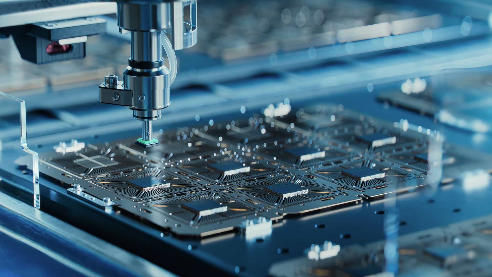
- Die Singulation & Inspection: Precision dicing of wafers into individual dies using blade and laser techniques; sorting of dies based on test results and quality grading; automated inspection for surface defects, cracks, and contamination.
- Wafer Grinding & Thinning: Backgrinding to achieve precise wafer thickness for integration and packaging; stress relief and surface conditioning; tape mounting and de-taping processes for safe handling.
- Lithography: Photolithography for pattern transfer using high-precision stepper/scanner systems; alignment and exposure for sub-micron accuracy; resist development and etching for functional layer creation.
- Laser Etching: Precision marking and structuring of wafers and dies; support for customized pattern creation and identification marking.
Services
- Custom Semiconductor Design: End-to-end design support for semiconductor devices; collaboration on architecture definition, RTL design, and IP integration.
- Packaging: Wafer-level packaging (WLP), flip-chip bonding, wire bonding; encapsulation and molding for environmental protection; thermal and mechanical reliability testing.
- Post-Silicon Validation: Silicon bring-up, functional testing, characterization of device performance; iterative feedback for design optimization before mass production.
- Prototyping & Validation: Rapid prototyping for design verification; FPGA emulation and test chip fabrication for proof-of-concept validation.
- Testing & Characterization: Electrical and parametric testing for yield analysis; reliability testing for temperature, vibration, long-term operation; compliance testing (JEDEC, IPC standards).
Core Applications
- High-Performance Computing (HPC): Custom chips and semiconductor components optimized for supercomputers, AI accelerators, and big data processing.
- Next-Generation Communication Systems: Semiconductor devices for 5G/6G, IoT connectivity, and advanced networking.
- Industrial Electronics: Components for rugged, high-reliability industrial systems.
- Consumer & Embedded Systems: Semiconductor solutions for embedded control, IoT modules, and smart devices.
- Defense & Aerospace: Radiation-hardened and ruggedized semiconductor components for mission-critical applications.
Value Proposition
- Full spectrum of wafer processing, design, packaging, and validation services.
- Deep expertise in semiconductor manufacturing processes and advanced lithography.
- Strong support for custom semiconductor design and prototype development.
- Commitment to high-quality, reliable, and scalable semiconductor solutions.
- End-to-end support from wafer to post-silicon testing, ensuring faster time-to-market.